Cypress NoBL CY7C1352G User Manual
Browse online or download User Manual for Unknown Cypress NoBL CY7C1352G. Cypress NoBL CY7C1352G User's Manual [pt]
- Page / 12
- Table of contents
- BOOKMARKS
Summary of Contents
4-Mbit (256K x 18) Pipelined SRAM withNoBL™ ArchitectureCY7C1352GCypress Semiconductor Corporation • 198 Champion Court • San Jose, CA 95134-1709 • 40
CY7C1352GDocument #: 38-05514 Rev. *D Page 10 of 12NOP, STALL, and DESELECT Cycles[18, 19, 21]ZZ Mode Timing[22, 23]Notes: 21.The IGNORE CLOCK EDGE or
CY7C1352GDocument #: 38-05514 Rev. *D Page 11 of 12© Cypress Semiconductor Corporation, 2006. The information contained herein is subject to change w
CY7C1352GDocument #: 38-05514 Rev. *D Page 12 of 12Document History PageDocument Title: CY7C1352G 4-Mbit (256K x 18) Pipelined SRAM with NoBL™ Archite
CY7C1352GDocument #: 38-05514 Rev. *D Page 2 of 12Selection Guide 250 MHz 200 MHz 166 MHz 133 MHz UnitMaximum Access Time 2.6 2.8 3.5 4.0 nsMaximum O
CY7C1352GDocument #: 38-05514 Rev. *D Page 3 of 12Pin DefinitionsName I/O DescriptionA0, A1, A Input-SynchronousAddress Inputs used to select one of t
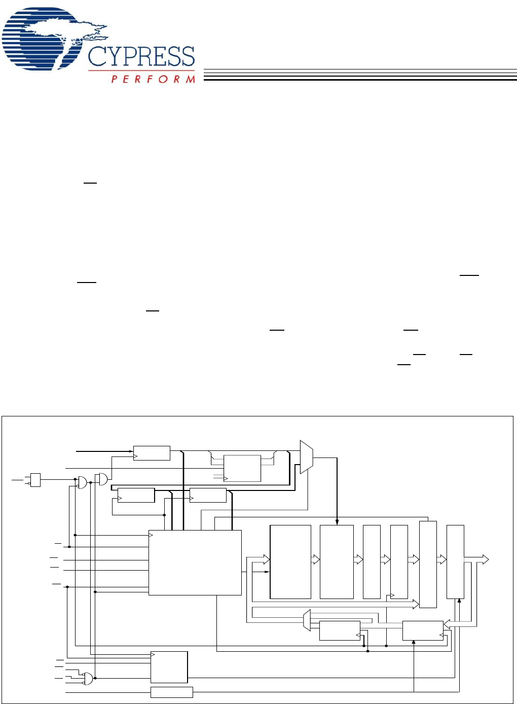
CY7C1352GDocument #: 38-05514 Rev. *D Page 4 of 12Functional OverviewThe CY7C1352G is a synchronous-pipelined Burst SRAMdesigned specifically to elimi
CY7C1352GDocument #: 38-05514 Rev. *D Page 5 of 12 Interleaved Burst Address Table (MODE = Floating or VDD)FirstAddressA1, A0SecondAddressA1, A0Third
CY7C1352GDocument #: 38-05514 Rev. *D Page 6 of 12Maximum Ratings(Above which the useful life may be impaired. For user guide-lines, not tested.)Stora
CY7C1352GDocument #: 38-05514 Rev. *D Page 7 of 12ISB4Automatic CEPower-down Current—TTL InputsVDD = Max, Device Deselected, VIN ≥ VIH or VIN ≤ VIL, f
CY7C1352GDocument #: 38-05514 Rev. *D Page 8 of 12Switching Characteristics Over the Operating Range[16, 17]Parameter Description–250 –200 –166 –133
CY7C1352GDocument #: 38-05514 Rev. *D Page 9 of 12Switching WaveformsRead/Write Timing[18, 19, 20]Notes: 18.For this waveform ZZ is tied low.19.When C
Related products and manuals for Unknown Cypress NoBL CY7C1352G
 (23 pages)
(16 pages)
(10 pages)
(12 pages)
(11 pages)
(23 pages)
(36 pages)
(38 pages)
(47 pages)
(31 pages)
(27 pages)
(36 pages)
(110 pages)
(31 pages)
(37 pages)
(82 pages)
(31 pages)
(28 pages)
(35 pages)
(23 pages)
(16 pages)
(10 pages)
(12 pages)
(11 pages)
(23 pages)
(36 pages)
(38 pages)
(47 pages)
(31 pages)
(27 pages)
(36 pages)
(110 pages)
(31 pages)
(37 pages)
(82 pages)
(31 pages)
(28 pages)
(35 pages)
© 2020, manymanuals.com. All rights reserved. | 0.849 s |
 Manymanuals.com
 Manymanuals.de
 Manymanuals.fr
 Manymanuals.it
 Manymanuals.pl
 Manymanuals.cz
 Manymanuals.es
 Manymanuals-pt.com
Comments to this Manuals