Cypress CY7C1470V25 User Manual
Browse online or download User Manual for Unknown Cypress CY7C1470V25. Cypress CY7C1470V25 User's Manual
- Page / 28
- Table of contents
- BOOKMARKS
- CY7C1470V25 1
- CY7C1472V25 1
- CY7C1474V25 1
- [+] Feedback 10
Summary of Contents
72-Mbit(2M x 36/4M x 18/1M x 72)Pipelined SRAM with NoBL™ ArchitectureCY7C1470V25CY7C1472V25CY7C1474V25Cypress Semiconductor Corporation • 198 Champi
CY7C1470V25CY7C1472V25CY7C1474V25Document #: 38-05290 Rev. *I Page 10 of 28IEEE 1149.1 Serial Boundary Scan (JTAG)The CY7C1470V25/CY7C1472V25/CY7C147
CY7C1470V25CY7C1472V25CY7C1474V25Document #: 38-05290 Rev. *I Page 11 of 28Instruction RegisterThree-bit instructions can be serially loaded into the
CY7C1470V25CY7C1472V25CY7C1474V25Document #: 38-05290 Rev. *I Page 12 of 28possible to capture all other signals and simply ignore thevalue of the CL
CY7C1470V25CY7C1472V25CY7C1474V25Document #: 38-05290 Rev. *I Page 13 of 282.5V TAP AC Test ConditionsInput pulse levels ...
CY7C1470V25CY7C1472V25CY7C1474V25Document #: 38-05290 Rev. *I Page 14 of 28 Scan Register SizesRegister Name Bit Size (x36) Bit Size (x18) Bit Size
CY7C1470V25CY7C1472V25CY7C1474V25Document #: 38-05290 Rev. *I Page 15 of 28Boundary Scan Exit Order (2M x 36)Bit # 165-Ball ID Bit # 165-Ball ID Bit
CY7C1470V25CY7C1472V25CY7C1474V25Document #: 38-05290 Rev. *I Page 16 of 28Boundary Scan Exit Order (1M x 72) Bit # 209-Ball ID Bit # 209-Ball ID Bit
CY7C1470V25CY7C1472V25CY7C1474V25Document #: 38-05290 Rev. *I Page 17 of 28Maximum Ratings (Above which the useful life may be impaired. For user gui
CY7C1470V25CY7C1472V25CY7C1474V25Document #: 38-05290 Rev. *I Page 18 of 28 Capacitance[14]Parameter Description Test Conditions100 TQFPMax.165 FBGAM
CY7C1470V25CY7C1472V25CY7C1474V25Document #: 38-05290 Rev. *I Page 19 of 28Switching Characteristics Over the Operating Range [15, 16]Parameter Descr
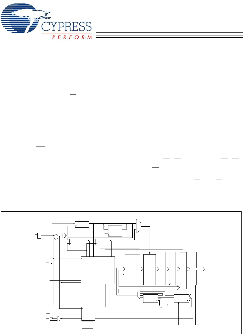
CY7C1470V25CY7C1472V25CY7C1474V25Document #: 38-05290 Rev. *I Page 2 of 28 A0, A1, ACMODEBWaBWbWECE1CE2CE3OEREAD LOGICDQsDQPaDQPbDATASTEERINGOUTPUT
CY7C1470V25CY7C1472V25CY7C1474V25Document #: 38-05290 Rev. *I Page 20 of 28Switching Waveforms Read/Write/Timing[21, 22, 23]Notes: 21. For this wavef
CY7C1470V25CY7C1472V25CY7C1474V25Document #: 38-05290 Rev. *I Page 21 of 28NOP, STALL and DESELECT Cycles[21, 22, 24]ZZ Mode Timing[25, 26]Notes: 24.
CY7C1470V25CY7C1472V25CY7C1474V25Document #: 38-05290 Rev. *I Page 22 of 28Ordering InformationNot all of the speed, package and temperature ranges a
CY7C1470V25CY7C1472V25CY7C1474V25Document #: 38-05290 Rev. *I Page 23 of 28250 CY7C1470V25-250AXC 51-85050 100-Pin Thin Quad Flat Pack (14 x 20 x 1.4
CY7C1470V25CY7C1472V25CY7C1474V25Document #: 38-05290 Rev. *I Page 24 of 28Package Diagrams NOTE:1. JEDEC STD REF MS-0262. BODY LENGTH DIMENSION DOES
CY7C1470V25CY7C1472V25CY7C1474V25Document #: 38-05290 Rev. *I Page 25 of 28Package Diagrams (continued)A1PIN 1 CORNER17.00±0.1015.00±0.107.001.00Ø0.
CY7C1470V25CY7C1472V25CY7C1474V25Document #: 38-05290 Rev. *I Page 26 of 28© Cypress Semiconductor Corporation, 2006. The information contained herei
CY7C1470V25CY7C1472V25CY7C1474V25Document #: 38-05290 Rev. *I Page 27 of 28Document History PageDocument Title: CY7C1470V25/CY7C1472V25/CY7C1474V25 7
CY7C1470V25CY7C1472V25CY7C1474V25Document #: 38-05290 Rev. *I Page 28 of 28*I 472335 See ECN VKN Corrected the typo in the pin configuration for 209-
CY7C1470V25CY7C1472V25CY7C1474V25Document #: 38-05290 Rev. *I Page 3 of 28Pin ConfigurationsAAAAA1A0VSSVDDAAAAAAVDDQVSSDQb DQb DQb VSSVDDQDQb DQb VSS
CY7C1470V25CY7C1472V25CY7C1474V25Document #: 38-05290 Rev. *I Page 4 of 28Pin Configurations (continued)234 5671ABCDEFGHJKLMNPRTDONC/576MNC/1GDQPcDQc
CY7C1470V25CY7C1472V25CY7C1474V25Document #: 38-05290 Rev. *I Page 5 of 28Pin Configurations (continued)ABCDEFGHJKLMNPRTUVW123456789 1110DQgDQgDQgDQg
CY7C1470V25CY7C1472V25CY7C1474V25Document #: 38-05290 Rev. *I Page 6 of 28ADV/LDInput-SynchronousAdvance/Load Input used to advance the on-chip addre
CY7C1470V25CY7C1472V25CY7C1474V25Document #: 38-05290 Rev. *I Page 7 of 28Functional OverviewThe CY7C1470V25/CY7C1472V25/CY7C1474V25 aresynchronous-p
CY7C1470V25CY7C1472V25CY7C1474V25Document #: 38-05290 Rev. *I Page 8 of 28CY7C1474V25, BWa,b,c,d for CY7C1470V25 and BWa,b forCY7C1472V25) inputs mus
CY7C1470V25CY7C1472V25CY7C1474V25Document #: 38-05290 Rev. *I Page 9 of 28Partial Write Cycle Description[1, 2, 3, 8]Function (CY7C1470V25) WE BWdBWc
Related products and manuals for Unknown Cypress CY7C1470V25
 (13 pages)
(10 pages)
(37 pages)
(32 pages)
(10 pages)
(32 pages)
(9 pages)
(6 pages)
(26 pages)
(31 pages)
(16 pages)
(14 pages)
(27 pages)
(29 pages)
(10 pages)
(22 pages)
(28 pages)
(14 pages)
(12 pages)
(13 pages)
(10 pages)
(37 pages)
(32 pages)
(10 pages)
(32 pages)
(9 pages)
(6 pages)
(26 pages)
(31 pages)
(16 pages)
(14 pages)
(27 pages)
(29 pages)
(10 pages)
(22 pages)
(28 pages)
(14 pages)
(12 pages)
© 2020, manymanuals.com. All rights reserved. | 0.080 s |
 Manymanuals.com
 Manymanuals.de
 Manymanuals.fr
 Manymanuals.it
 Manymanuals.pl
 Manymanuals.cz
 Manymanuals.es
 Manymanuals-pt.com
Comments to this Manuals